Inverter Scheme
Article Category: Household appliances field
Release time: 2023-10-23 10:17:07
Number of page views: 9662
Share:
-
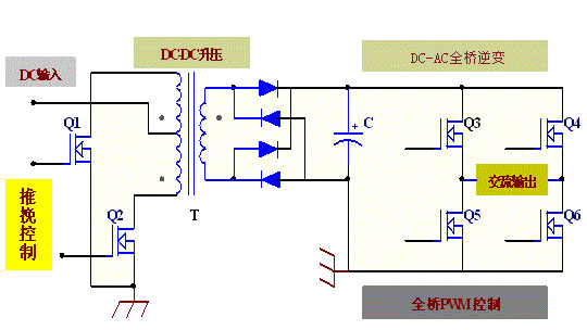
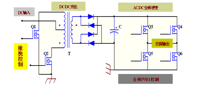
Recommendation for use: For the front-end DC-DC boost in this scheme, a push-pull circuit is recommended, and the switch transistors Q1/Q2 are recommended to be selected according to different input voltages. The recommended MOSFET models are as follows:
The BVDSS requirement of the MOSFET varies with different input voltages.
Input Voltage
BVDSS Requirement of MOSFET
Recommended Feihong model:
12V
40-60V
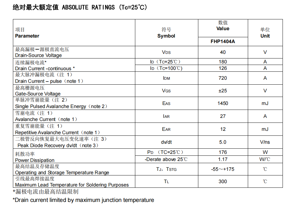
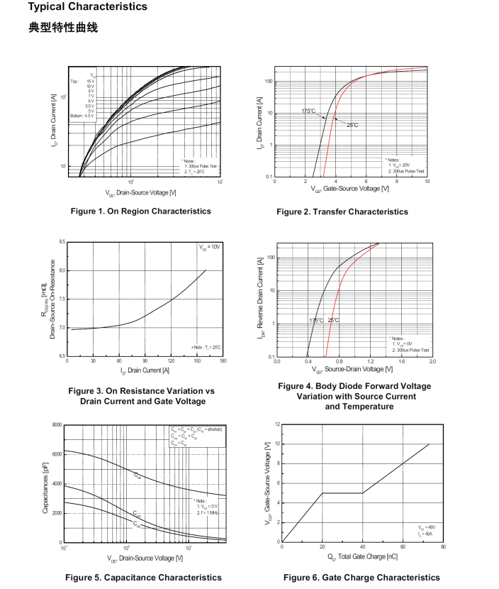
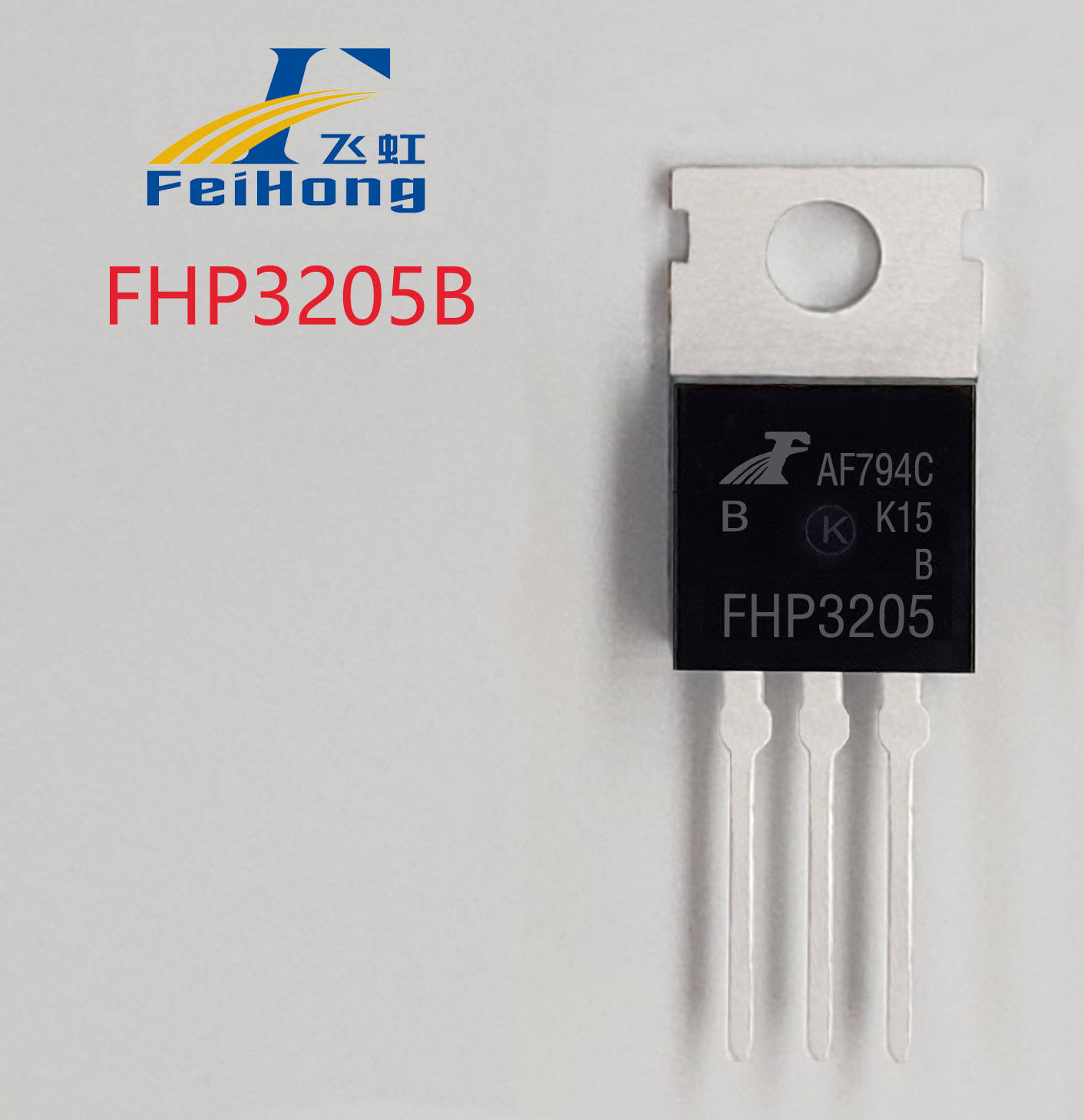
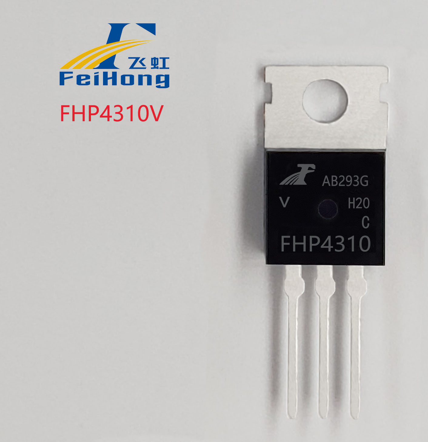
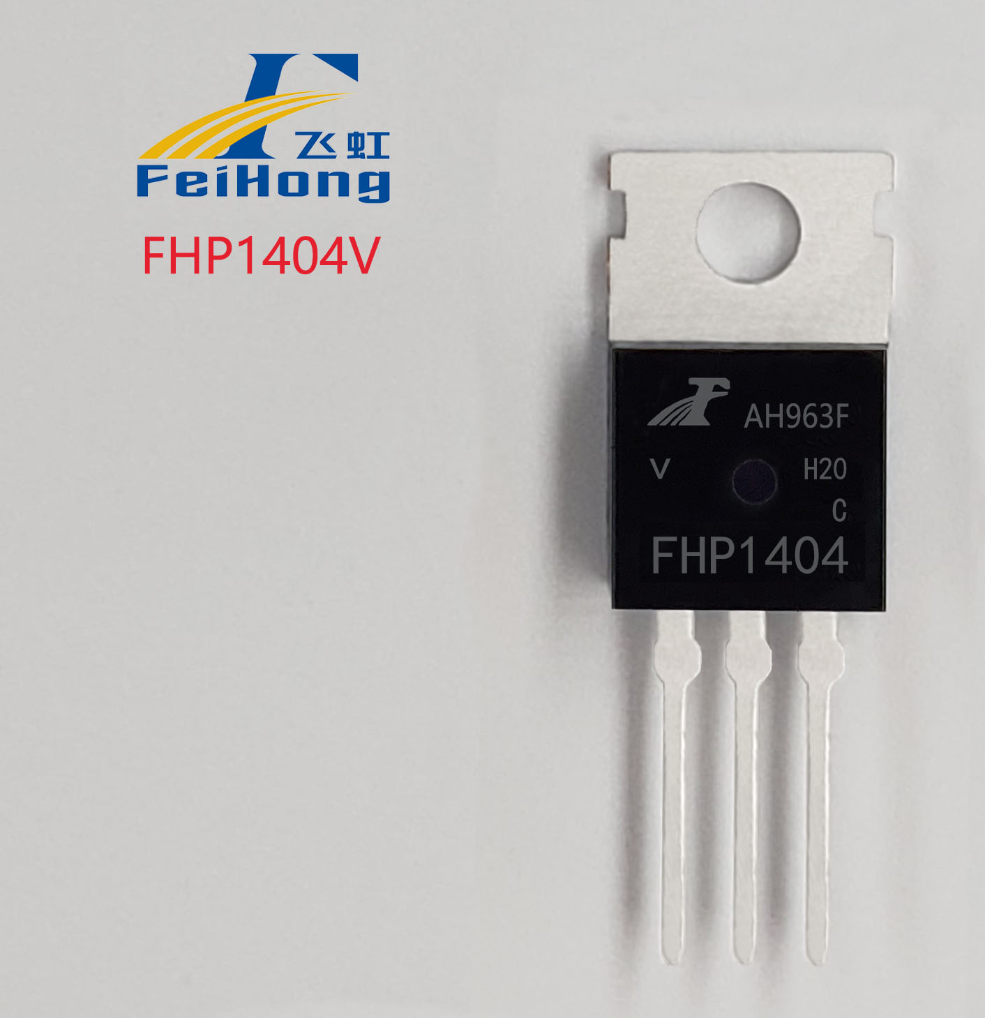
1404, 50N06, 3205, 80N07, 100N07
24V
80V
70N08, 80N08, 100N08
36V
90-110V
530, 540, 3710, 75N100, 4410
48V
120-200V
630, 640, 40N20
For the back-end AC-DC full bridge inverter circuit, based on different output voltage requirements in different markets such as Asia and North America, the main typical output voltage values of the inverter's back-end are summarized as 110V and 220V;
the output waveform of the inverter mainly consists of square waves and sine waves. The selection of MOSFETs for Q3~Q6 can refer to the table below.
Output Voltage
BVDSS Requirement of MOSFET
Recommended Feihong model:
110V (Square Wave)
200V
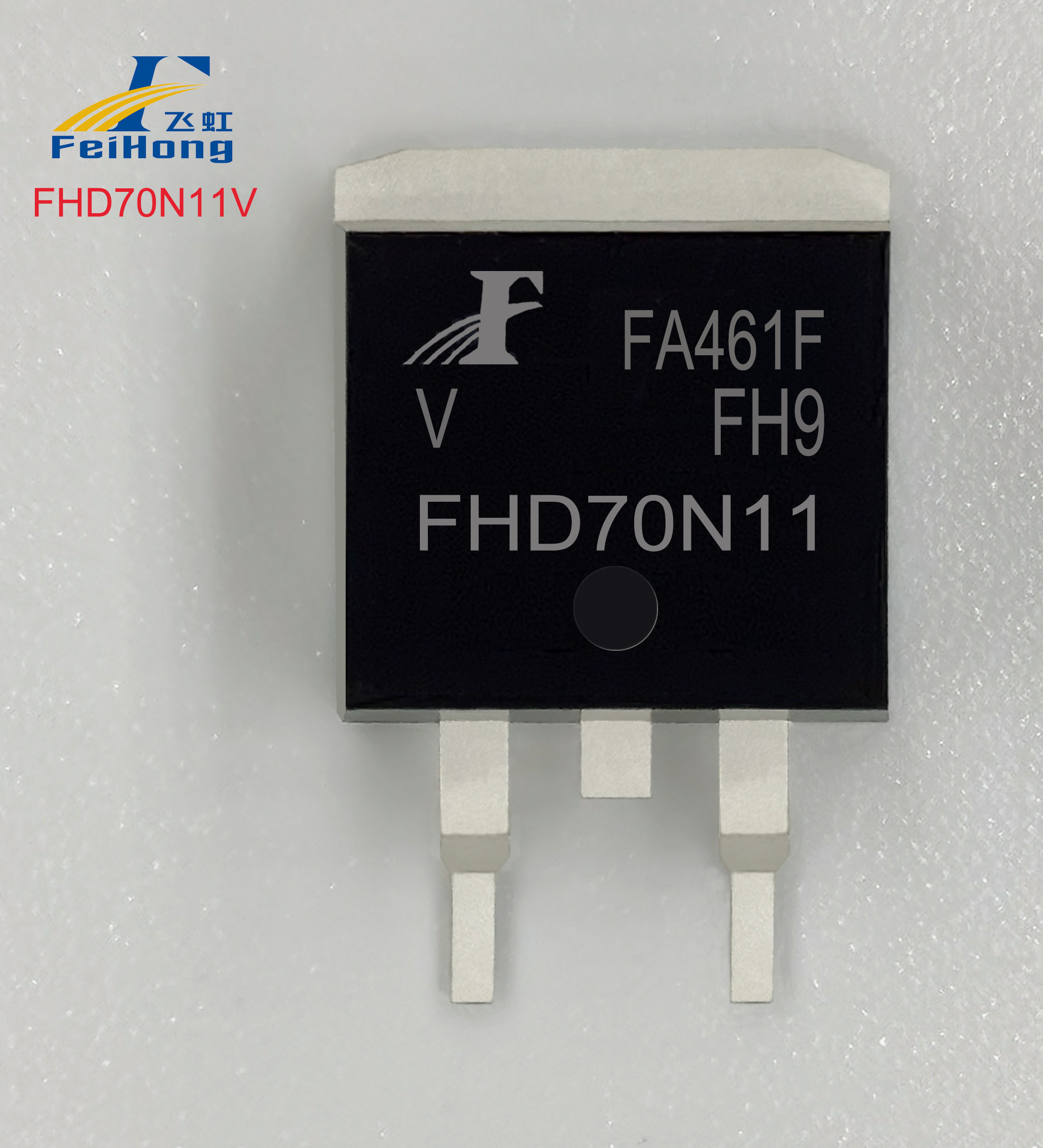
630, 640, 40N20
110V (Sine Wave)
400V
730, 740, 20N40, 830, 840, 13N50, 20N50, etc.
220V (Square Wave)
400V
730, 740, 20N40
220V (Sine Wave)
600V
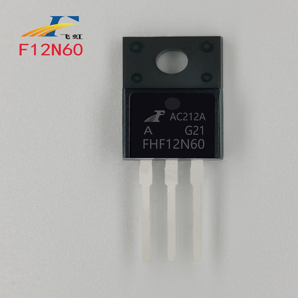
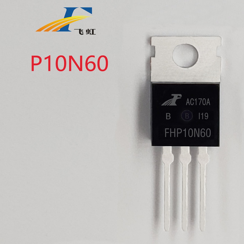
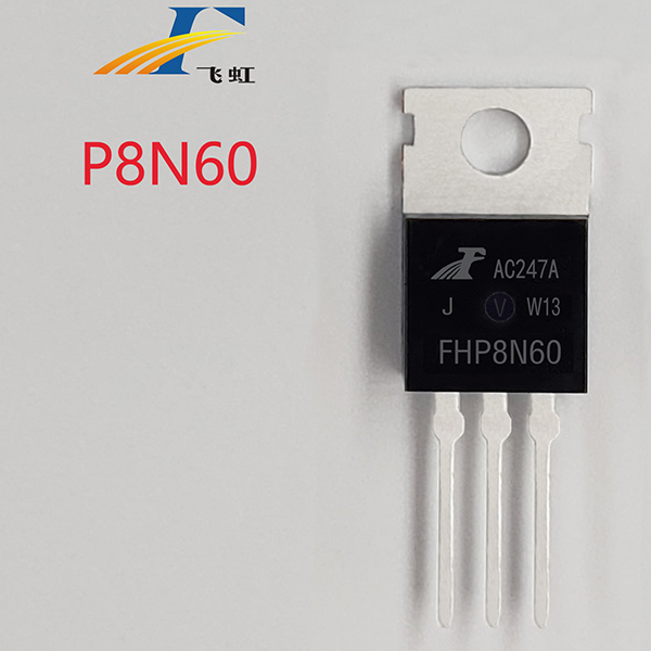
8N60, 10N60, 12N60, 15N60, 20N60, etc.
-
Associated Scheme Products
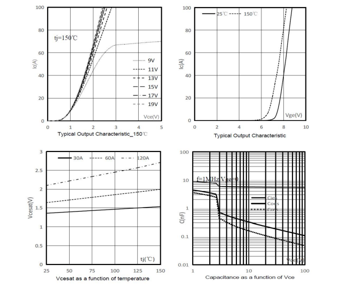
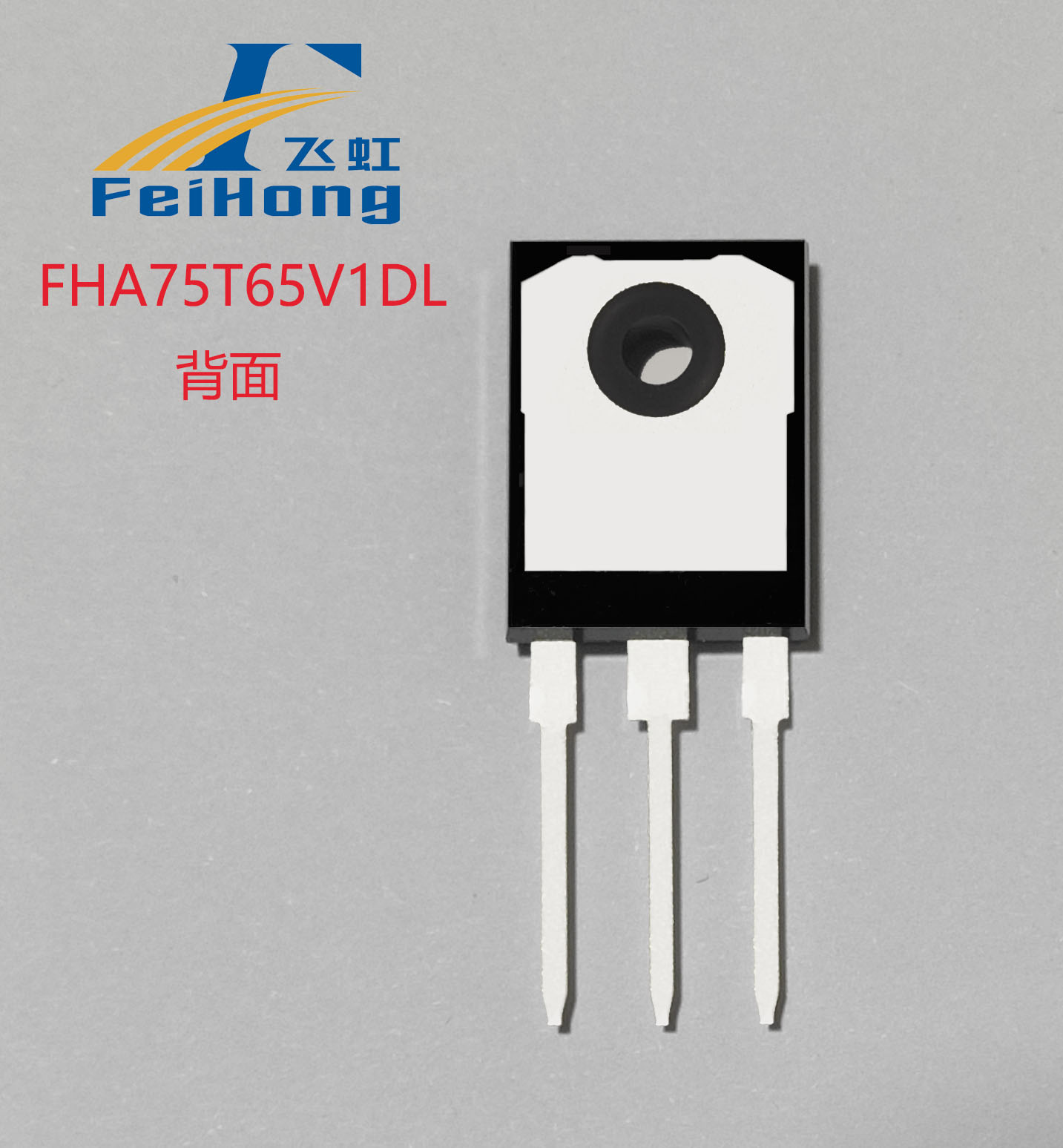
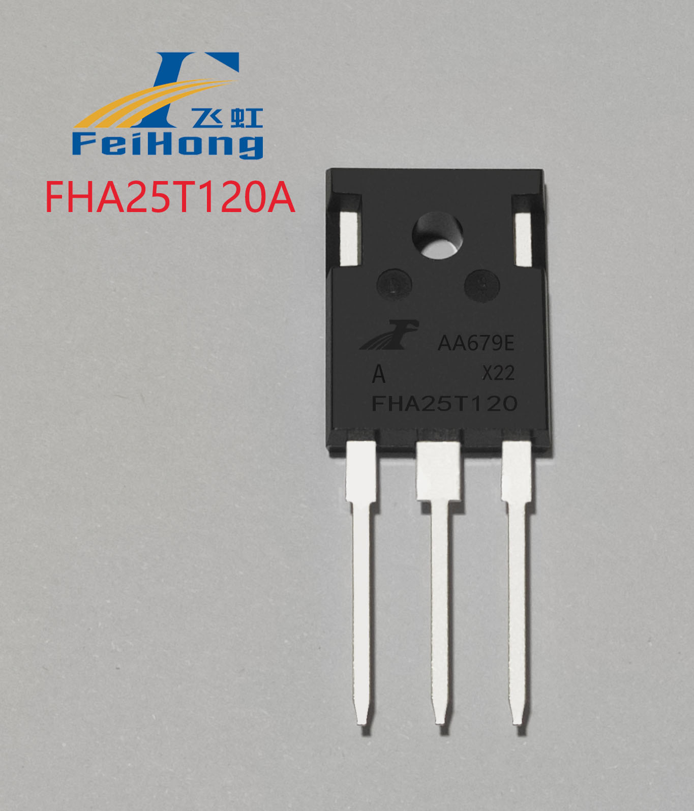
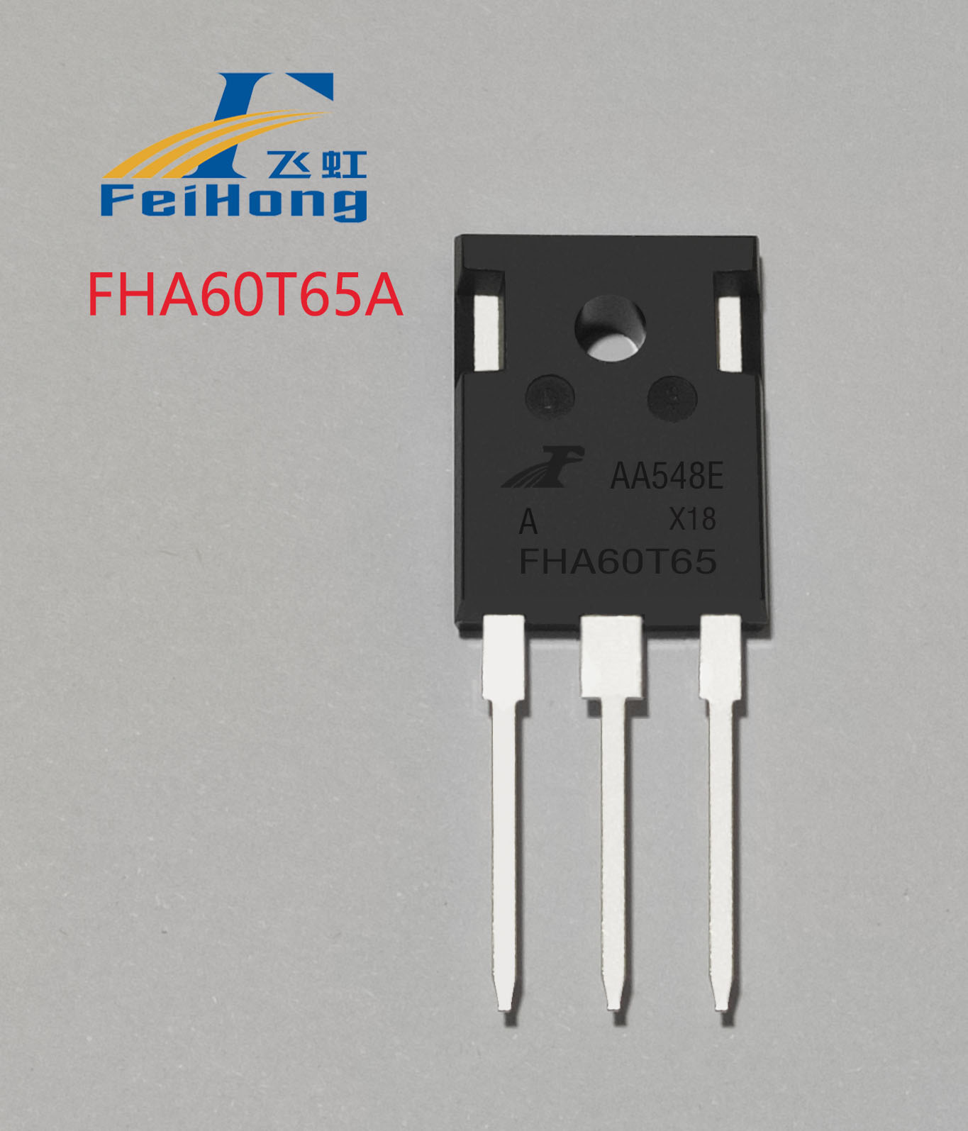
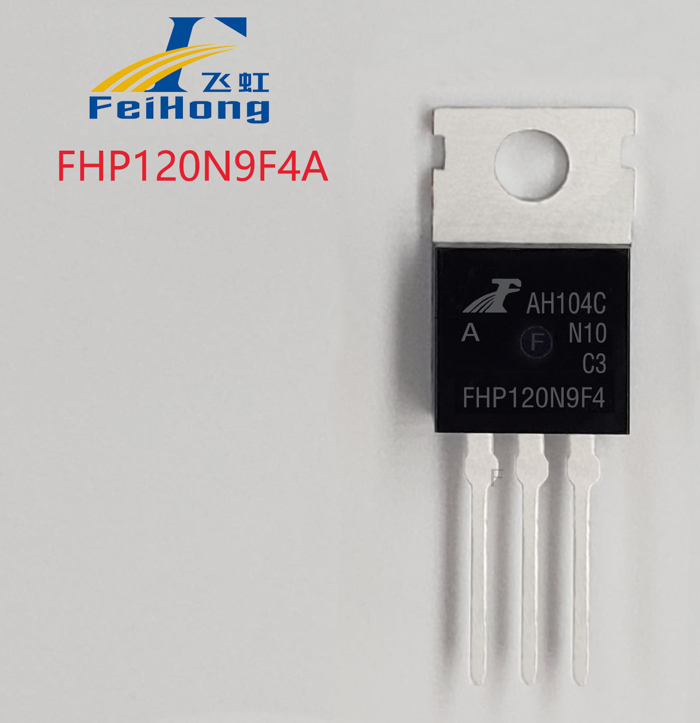
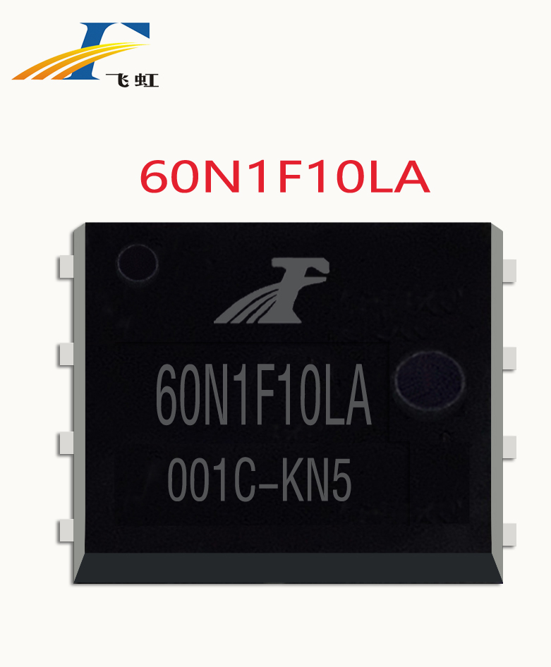
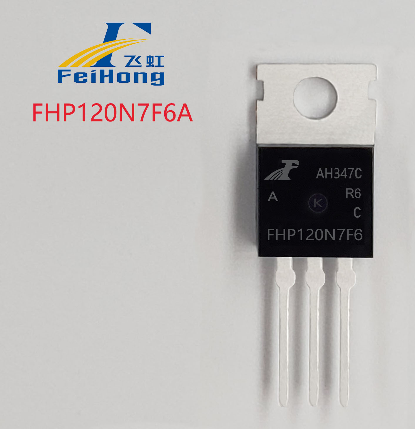
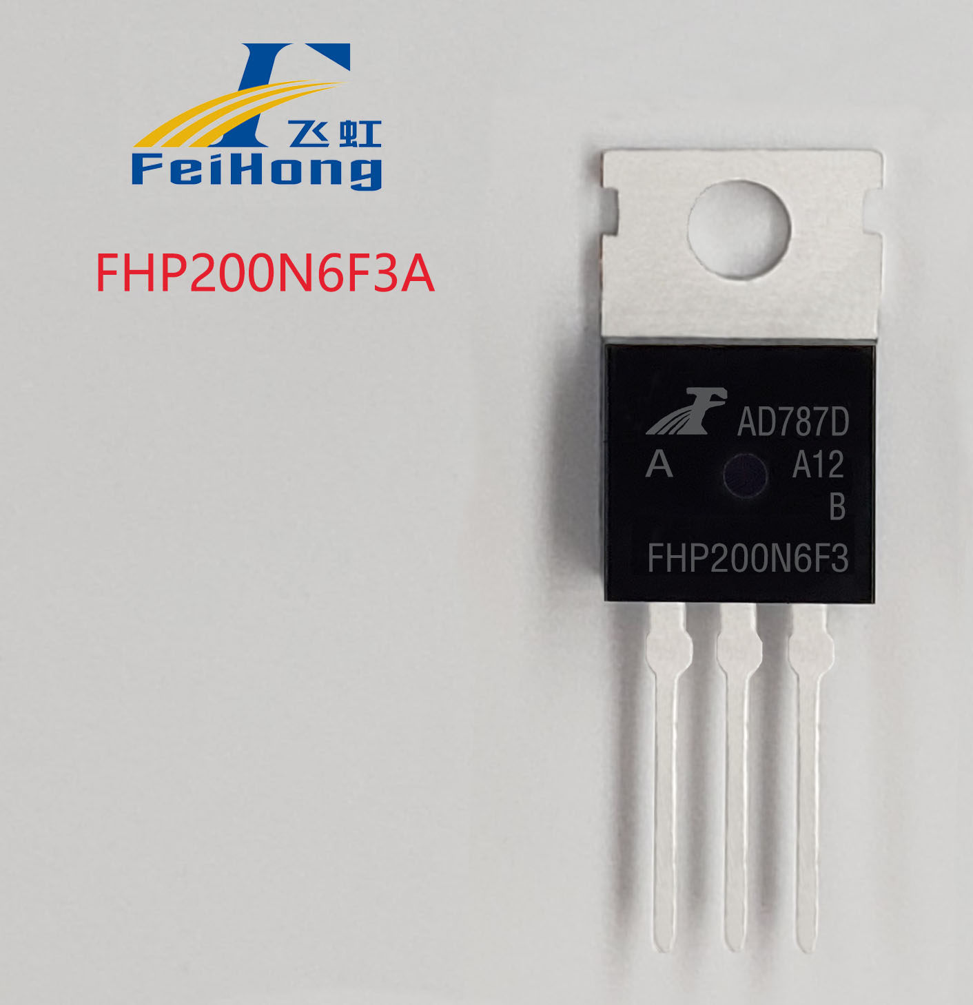
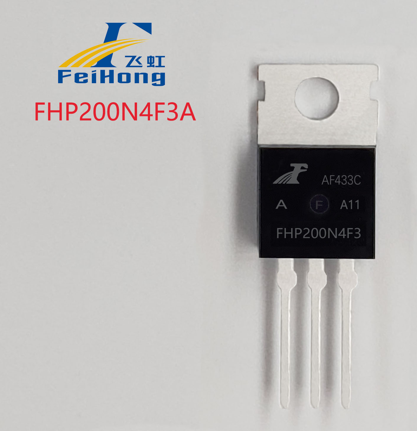
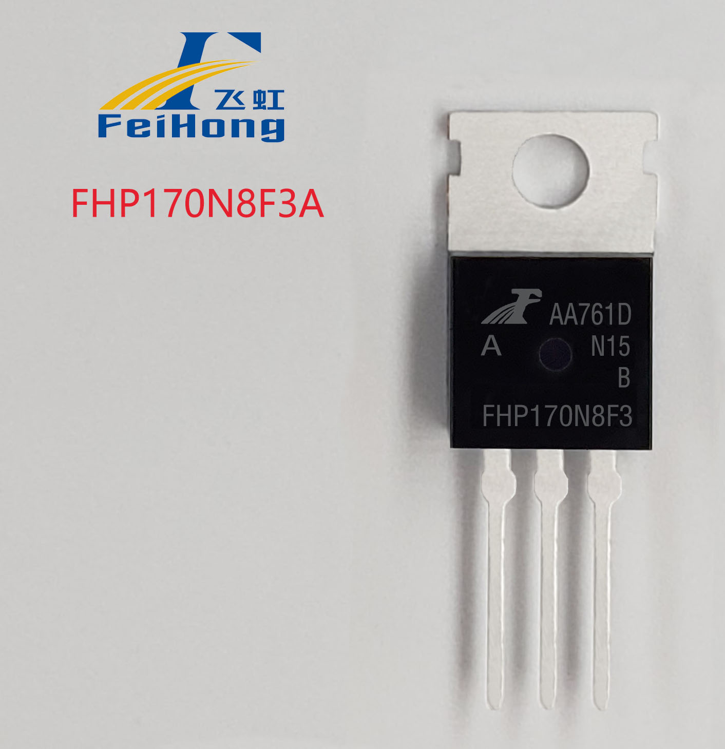
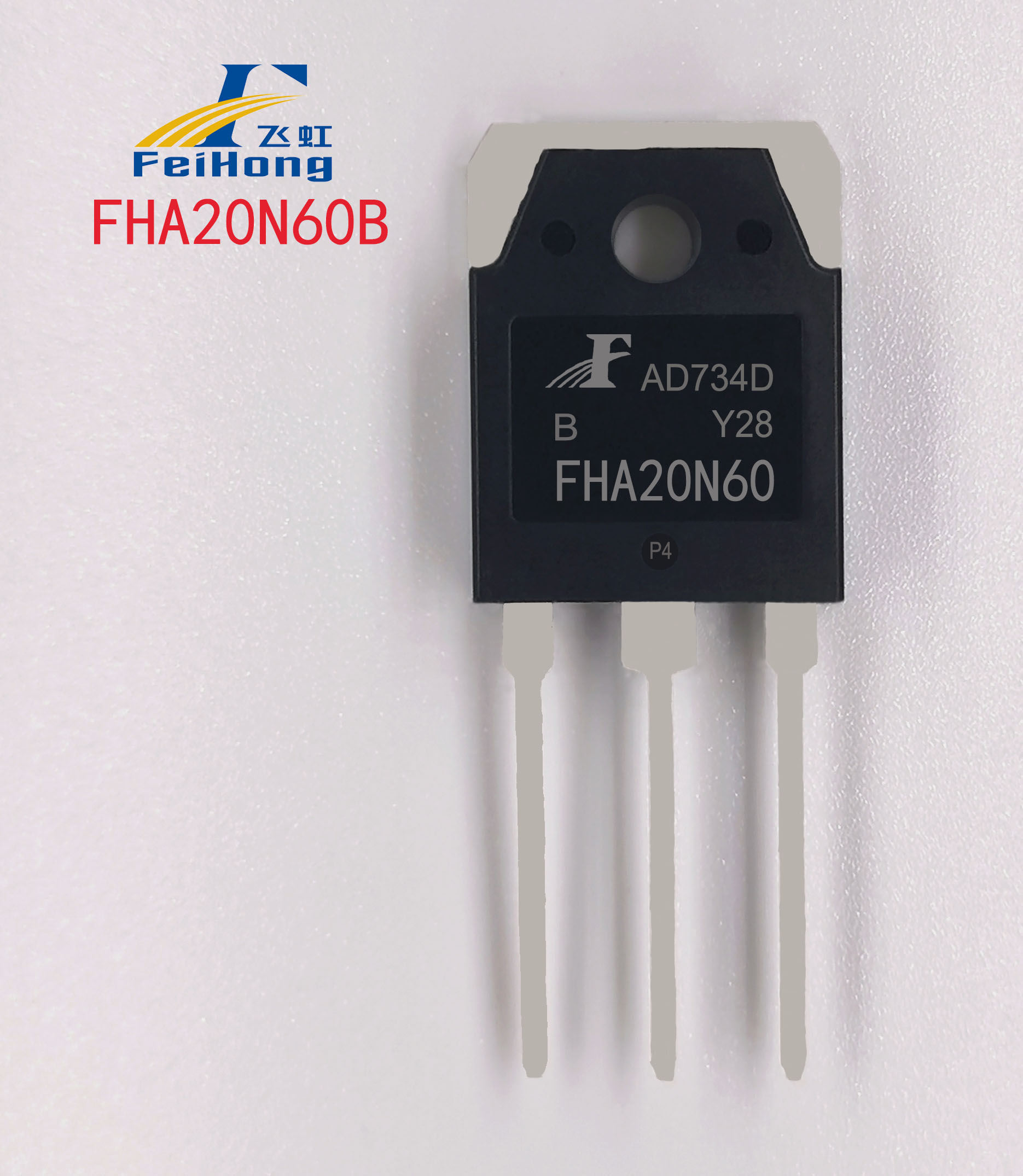
Part Number Polarity Package Vgs(±V) VTH(V) ID(A) BVdss(V) Rds(on)(mΩ) Model Polarity Encapsulation form Vgs=10v(typ) Vgs=10v(max) Vgs=4.5v(typ) Vgs=4.5v(max) Part Number Polarity Package Vgs(±V) VTH(V) ID(A) BVdss(V) Rds(on)(mΩ) Model Polarity Encapsulation form Vgs=10v(typ) Vgs=10v(max) FHP540C/FHD540C N TO-220 TO-252 30 2~4 33 100 37 44 FHP1404 N TO-220 25 2-4 180 40 2.5 3.3 FHP3205D N TO-220 20 2~4 110 55 7.5 8.5 FHP3710C N TO-220 20 2~4 57 100 18 23 FHP20N40W N TO-220 30 2~4 20 400 0.22 0.27 FHP20N50B/FHF20N50B/FHA20N50B N TO-220 TO-220F TO-3PN/247 30 2~4 20 500 0.23 0.28 FHP40N20D N TO-220 30 2~4 40 200 0.05 0.065 FHP630A/FHF630A/FHD630A N TO-220 TO-220F TO-252 30 2~4 9 200 0.3 0.4 FHP640A N TO-220 30 2~4 18 200 0.125 0.18 FHP730B N TO-220 30 2~4 6 400 0.75 0.9 FHP740W N TO-220 30 2~4 10 400 0.38 0.5 FHP830C/FHD830C N TO-220 TO-252 30 2~4 5 500 1.51 1.6 FHP840/FHF840 N TO-220/TO-220F 30 2-4 9 500 - 0.8 FHP10N60D/FHF10N60D N TO-220 TO-220F 30 2~4 10 600 0.67 0.8 FHP8N60B/FHF8N60B N TO-220 TO-220F 30 2~4 8 600 1 1.15 FHP20N60B/FHF20N60B/FHA20N60B N TO-220 TO-220F TO-3PN/247 30 2~4 20 600 0.32 0.4 FHP13N50W/FHF13N50W N TO-220 TO-220F 30 2~4 13 500 0.36 0.45 FHP20N50W/FHF20N50W/FHA20N50W N TO-220 TO-220F TO-3PN/247 30 2~4 20 500 0.22 0.27 FHP8N60W/FHF8N60W N TO-220 TO-220F 30 2~4 8 600 0.9 1.15 Part Number Polarity Package Vgs(±V) VTH(V) ID(A) BVdss(V) Rds(on)(mΩ) Model Polarity Encapsulation form Vgs=10v(typ) Vgs=10v(max) Vgs=4.5v(typ) Vgs=4.5v(max) FHP50N06B/FHD50N06B/FHU50N06B N TO-220 TO-252 TO-251 20 2~4 75 60 8.5 10.5 FHP80N07L N TO-220 20 1~2.5 80 60 8.4 11 9.5 13 FHP80N08B/FHS80N08B N TO-220 TO-263 20 2~4 90 80 6.8 8 FHP100N07B/FHS100N07B N TO-220 TO-263 20 2~4 100 68 5.9 7.2 FHP100N08B/FHD100N08B N TO-220 TO-252 20 2~4 100 80 6 7.2 FHP80N07L N TO-220 20 1~2.5 80 60 8.4 11 9.5 13 FHP80N07L1 N TO-220 20 1~2.5 75 60 8.4 11 12.4 14.5 FHP80N07G/FHS80N07G/FHD80N07G N TO-220 TO-263 TO-252 20 2~4 75 68 7.4 8.5 FHP80N07E/FHS80N07E/FHD80N07E N TO-220 TO-263 TO-252 20 2~4 80 68 7.1 8.5 FHP3205C/FHD3205C N TO-220 TO-252 20 2~4 130 68 4.6 5.4 FHP80N08B/FHS80N08B N TO-220 TO-263 20 2~4 90 80 6.8 8 FHD80N08C N TO-252 20 2~4 80 80 8.1 9.3 FHP100N08B/FHD100N08B N TO-220 TO-252 20 2~4 100 80 6 7.2 FHP540E/FHD540E N TO-220 TO-252 20 2~4 37 100 22.5 28 Part Number Polarity Package Vgs(±V) VTH(V) ID(A) BVdss(V) Rds(on)(mΩ) With FRD Diode Model Polarity Encapsulation form Vgs=10v(typ) Vgs=10v(max) Part Number Package VGE(th)(V) IC-100℃(A) BVCES(V) VCESAT(V) VF(V) Model Encapsulation form typ max typ Part Number Polarity Package PIN Ic(A) BVCEO(V) BVCBO(V) hFE Model Polarity Encapsulation form Foot arrangement min max 2N5401 PNP TO-92 EBC -0.5 -150 -160 60 240 Part Number Package PIN VRRM(V) VF(V) IR(uA) IF(A) junction temperatureTj(℃) Model Encapsulation form Foot position typ max max Single Whole Part Number Package PIN Iout(A) Vout(V) VI(V) Model Encapsulation form Foot arrangement min max Part Number Package peak reverse voltage Forward currentIF(AV)(A) Forward conduction voltage dropVF(V) reverse recoveryTrr(ns) Model Encapsulation form VRRM(V) Single chip Dual chip typ max typ max










 Search
 LED Driver Selection Substitute Daquan recommend
